
Deep Learning Mini Projects
October 23, 2026
VLSI Projects for Students
October 23, 2026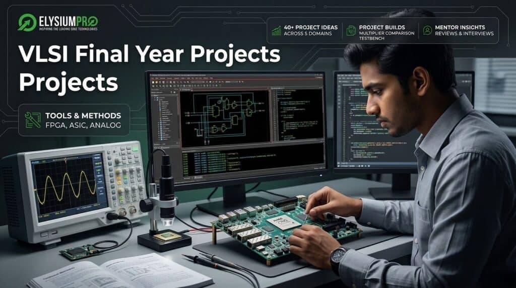
Introduction
Every smartphone, satellite and AI server runs on chips designed by VLSI engineers. With India building its own semiconductor ecosystem, that work is no longer happening only abroad. As a result, VLSI final year projects have become one of the strongest launchpads for ECE and EEE careers.
However, many students struggle to pick a VLSI topic. Some choose a simple adder that examiners have seen a hundred times. Others aim for a full processor and run out of time before verification.
This guide helps you choose wisely. You will learn which tools to use, whether to pick an FPGA, ASIC or analog project, 40 VLSI final year project ideas across five domains, and a complete multiplier comparison build with a self-checking testbench. Along the way, the mentors at Elysiumpro share what makes VLSI projects stand out in reviews and interviews.
What Are VLSI Final Year Projects?
VLSI final year projects are capstone projects in which students design, verify and implement integrated-circuit logic or analog blocks, then measure their area, timing and power. Most use Verilog, VHDL or SystemVerilog for digital design, or SPICE simulation for analog circuits. In short, they prove you can think like a chip designer.
- At a glance: the main VLSI design flows
- FPGA flow: RTL design, simulation, synthesis, implementation and testing on a real FPGA board.
- ASIC front-end: RTL design, verification, synthesis and static timing analysis.
- ASIC back-end: Floorplanning, placement, clock tree synthesis, routing and sign-off, often called RTL-to-GDSII.
- Analog and mixed-signal: Transistor-level circuit design, SPICE simulation and layout.
- Key metrics: Area (LUTs or µm²), delay or maximum frequency, power and verification coverage.
Which Tools Do You Need?
You need a simulator, a synthesis tool and, depending on your project, an FPGA toolchain, a physical design flow or a SPICE simulator. Both free and commercial options exist.
| Task | Free or open-source options | Commercial or academic options |
|---|---|---|
| RTL simulation | Icarus Verilog, Verilator, GHDL | ModelSim/Questa, Xcelium, VCS |
| Waveform viewing | GTKWave | Built-in tool viewers |
| Synthesis | Yosys | Vivado, Quartus, Design Compiler, Genus |
| FPGA implementation | Vendor free editions (Vivado ML Standard, Quartus Lite) | Full vendor editions |
| Static timing analysis | OpenSTA | PrimeTime, Tempus |
| RTL-to-GDSII | OpenLane or OpenROAD with SkyWater 130 nm PDK | Cadence Innovus, Synopsys IC Compiler |
| Analog simulation and layout | ngspice, Xschem, Magic | Cadence Virtuoso, Spectre |
| Formal verification | SymbiYosys | JasperGold, VC Formal |
Why Choose VLSI for Your Final Year Project?
Choose VLSI for your final year project because India's semiconductor industry is growing fast, chip-design roles value hands-on RTL and verification skills, and free tools now make complete design flows accessible. VLSI projects also lead naturally to M.Tech and research opportunities.
Should You Choose an FPGA, ASIC or Analog Project?
Choose an FPGA project for a hands-on demo, an ASIC-flow project for research on area and power, or an analog project if you enjoy transistor-level design. The table below compares the three.
| Factor | FPGA project | ASIC-flow project | Analog / mixed-signal project |
|---|---|---|---|
| Typical output | Working hardware demo | Synthesis, timing and layout reports | SPICE results and layout |
| Hardware cost | Development board (a few thousand rupees upwards) | None (software flow) | None (software flow) |
| Key skills | RTL, timing, interfacing | RTL, synthesis, STA, physical design | Device physics, circuit design |
| Demo impact | Very high | Medium (layout screenshots) | Medium (waveforms) |
| Research angle | Throughput, resource use | Area, power, timing trade-offs | Noise, gain, power, variation |
| Best for | ECE students targeting FPGA and embedded roles | Students targeting design or physical design roles | Students targeting analog or M.Tech research |
What Are the Best VLSI Final Year Projects for 2026?
The best VLSI final year projects for 2026 combine a meaningful design with a clear comparison or optimisation and measured results. Here are 40 ideas across five domains, each with a typical flow and level.
Digital arithmetic and DSP projects
| Project | Typical flow | Level |
|---|---|---|
| Array vs Wallace vs Booth multiplier comparison | FPGA plus OpenLane | Intermediate |
| Approximate multiplier for image processing | FPGA or ASIC flow | Advanced |
| Ripple, carry-select and Kogge-Stone adder comparison | FPGA or ASIC flow | Beginner |
| Vedic multiplier design and comparison | FPGA | Beginner |
| FIR filter using distributed arithmetic | FPGA | Intermediate |
| CORDIC unit for sine and cosine | FPGA | Intermediate |
| 64-point pipelined FFT processor | FPGA | Advanced |
| IEEE 754 single-precision floating-point adder | FPGA or ASIC flow | Advanced |
Low-power and physical design projects
| Project | Typical flow | Level |
|---|---|---|
| Ring oscillator frequency versus supply voltage | ngspice | Beginner |
| Pipelined versus non-pipelined timing study | Yosys and OpenSTA | Intermediate |
| Clock gating for dynamic power reduction | ASIC flow | Intermediate |
| Low-power CMOS comparator layout | Magic and ngspice | Intermediate |
| 6T versus 8T SRAM cell stability and power | ngspice | Advanced |
| RTL-to-GDSII of a 32-bit ALU | OpenLane with SkyWater 130 nm | Advanced |
| Power gating with state retention | ASIC flow | Advanced |
| Multi-threshold voltage optimisation study | ASIC flow | Advanced |
Verification and testing projects
| Project | Typical flow | Level |
|---|---|---|
| Self-checking testbench for an ALU | Simulation | Beginner |
| SystemVerilog assertions for a FIFO | Simulation | Intermediate |
| Functional coverage for a UART | Simulation | Intermediate |
| Memory BIST using March C- algorithm | FPGA or simulation | Intermediate |
| Stuck-at fault simulation | Simulation | Intermediate |
| UVM testbench for an APB slave | Simulation (UVM) | Advanced |
| Scan-chain insertion and ATPG study | ASIC flow | Advanced |
| Formal verification of a round-robin arbiter | SymbiYosys | Advanced |
Hardware security and AI accelerator projects
| Project | Typical flow | Level |
|---|---|---|
| Ring-oscillator PUF on FPGA | FPGA | Intermediate |
| True random number generator | FPGA | Intermediate |
| Lightweight crypto core (PRESENT or ASCON) | FPGA or ASIC flow | Intermediate |
| Hardware Trojan detection using side-channel features | Simulation and ML | Advanced |
| Systolic-array matrix multiplier for CNNs | FPGA | Advanced |
| Binarised neural network accelerator | FPGA | Advanced |
| Posit arithmetic unit versus IEEE float | FPGA or ASIC flow | Advanced |
| Spiking neuron hardware model | FPGA | Advanced |
How Do You Build and Verify a VLSI Design Step by Step?
Build and verify a VLSI design by writing clean RTL, testing it with a self-checking testbench, synthesising it for an FPGA or standard-cell library, analysing timing and power, and then comparing it against alternative architectures. The worked example below follows this flow.
Worked example: comparing three 8-bit multiplier architectures
A team of three final year ECE students wants to know which multiplier architecture gives the best balance of speed, area and power. They follow six steps.
- Write the RTL: Implement an array multiplier, a Wallace tree multiplier and a radix-4 Booth multiplier in Verilog.
- Verify exhaustively: Test every one of the 65,536 input combinations with a self-checking testbench in Icarus Verilog.
- Synthesise for FPGA: Use Vivado for an Artix-7 board and record LUT use, critical-path delay and estimated power.
- Run an ASIC flow: Use OpenLane with the SkyWater 130 nm PDK to compare cell area and timing.
- Analyse trade-offs: Plot area against delay and identify the best design for each goal.
- Demonstrate on hardware: Show results on the FPGA board using switches and a seven-segment display.
The self-checking testbench compares each design against the built-in multiplication operator:
`timescale 1ns/1ps
module tb_mult8;
reg [7:0] a, b;
wire [15:0] p;
reg [15:0] expected;
integer i, j, errors;
wallace_mult8 dut (.a(a), .b(b), .p(p)); // design under test
initial begin
errors = 0;
for (i = 0; i < 256; i = i + 1) begin
for (j = 0; j < 256; j = j + 1) begin
a = i; b = j;
expected = a * b;
#1;
if (p !== expected) begin
errors = errors + 1;
$display("Mismatch: %0d x %0d = %0d (expected %0d)", a, b, p, expected);
end
end
end
$display("Exhaustive test complete: %0d errors", errors);
$finish;
end
endmodule
Swap the module name to reuse the same testbench for the array and Booth designs.
Illustrative results
| Architecture | FPGA LUTs | Critical-path delay | Relative dynamic power | ASIC cell area (sky130) |
|---|---|---|---|---|
| Array multiplier | ~110 | ~9.5 ns | 1.00 (reference) | Smallest |
| Wallace tree | ~120 | ~6.8 ns | ~1.10 | Medium |
| Radix-4 Booth with Wallace tree | ~100 | ~6.2 ns | ~0.90 | Medium |
These figures are illustrative and will vary with tools and settings. However, they show what examiners reward: exhaustive verification, measurements from both FPGA and ASIC flows and a clear explanation of why each architecture behaves as it does.
How Do You Plan VLSI Final Year Projects Review by Review?
Plan VLSI final year projects by matching each review to a design milestone: specification first, verified RTL next, then synthesis and timing results, and finally optimisation, hardware demo and documentation.
| Review | Typical weeks | VLSI deliverables |
|---|---|---|
| Zeroth review | 1–3 | Title, base paper, block diagram, target metrics and tool choice |
| Review 1 | 5–7 | Literature survey, micro-architecture, first RTL modules |
| Review 2 | 10–13 | Complete RTL with self-checking testbench and waveforms |
| Review 3 | 16–18 | Synthesis, timing, power and area results, comparison with baseline |
| Final viva | 19–20 | FPGA demo or layout, report, presentation, backup video |
What Mistakes Should You Avoid?
Most problems in VLSI final year projects come from weak verification, unrealistic scope and missing measurements rather than from tool issues. Avoid these mistakes:
- Skipping verification: A design that "looks right" in one waveform is not verified.
- Over-scoping: A full out-of-order processor rarely fits a semester; a well-verified RV32I core does.
- Writing unsynthesisable RTL: Avoid delays and initial blocks in design code, and check synthesis warnings.
- Ignoring timing: Report the maximum frequency and fix negative sla
- No baseline comparison: Compare your design with a standard architecture.
- Reporting tool output without explanation: Explain why area, delay or power changed.
- No hardware or layout evidence: Include board photos, layout screenshots or a demo video.
Where Can You Get Expert Guidance?
You can get guidance from faculty, VLSI labs, open-source hardware communities and specialist mentors. Resources such as the OpenLane and OpenROAD documentation, NPTEL VLSI courses and vendor tutorials for Vivado and Quartus are excellent starting points.
For a complete capstone, structured mentoring helps you choose a realistic architecture, build strong testbenches and interpret tool reports. For example, Elysiumpro mentors VLSI academic projects, covering title selection, RTL and verification training, FPGA implementation and documentation while students design and verify the circuits themselves. Whichever route you choose, make sure you can explain every block of your design.
Conclusion
VLSI final year projects succeed when they combine clean design, rigorous verification and honest measurement. Choose between FPGA, ASIC and analog flows based on your goals, pick an idea with a clear comparison and verify it thoroughly. Then report area, timing and power, and explain the trade-offs.
In short, a verified, measured design beats an ambitious one that never closes timing. If you want guidance turning one of these 40 ideas into a high-scoring capstone, connect with the VLSI mentors at Elysiumpro and start designing today.